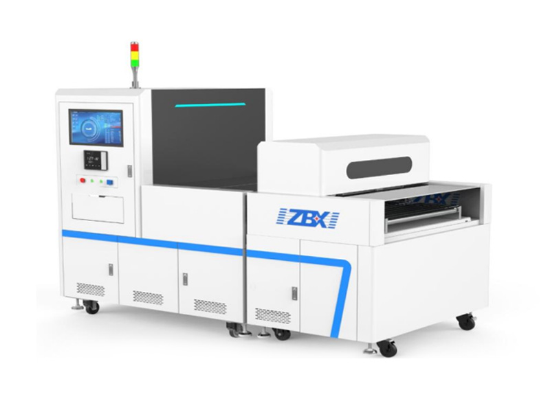
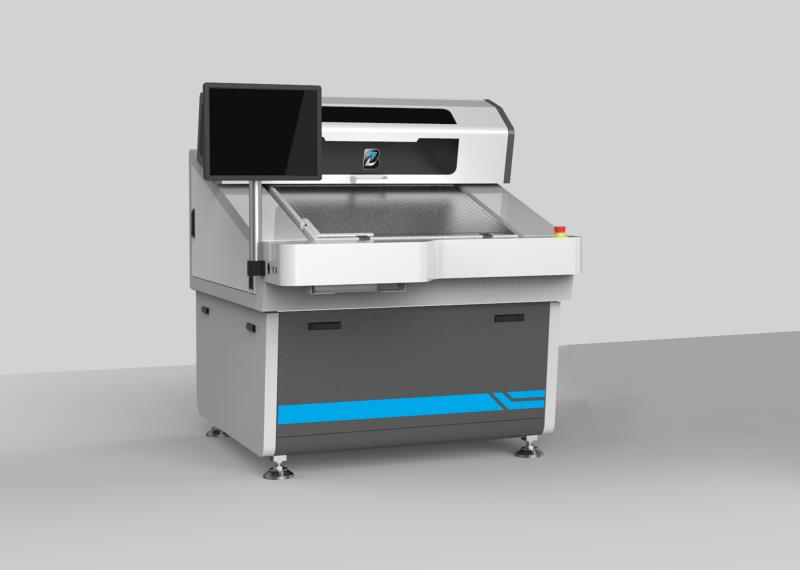
Online AOI testing system--Unique 9018

Online AOI testing system--Unique 9018
•It adopts an advanced system autonomous learning method and a high-precision visual imaging system to achieve sub-pixel level Analysis, can accurately detect small defects and filter unnecessary false defects
•High detection ability
•Low false detection ability
•VRS with high production capacity
Brief introduction
The automatic optical inspection ( AOI ) is used in the production process to identify the defects in PCB layers,then repair those defects through VRS, or remove them from production line.
The defects detected by AOI helps prevent those defective boards from being processed into the final process. It is of great value in terms of quality, process control, and yield improvement. It is a powerful mid-inspection assistant for PCB manufacturers.
assistant for PCB manufacturers.
Machine Features:
* Intelligent data analysis module greatly reduces the work time of data configuration.
* Supports mixing materials and automatically identifies material names.
* Multi-angle adjustable adaptive light source, adaptable to PCBs with many different board materials.
* Crawler-type conveying plate, double-sided simultaneous inspection, high detection efficiency,and more stable plate conveying.
* Online feeding and discharging (supports manual loading and unloading).
* Automatic inkjet printing, automatic whole board alignment, automatic focusing.
* Supports output of OK/NG board signal (can be connected to automatic board splitter).
* AI re-inspection system that supports artificial intelligence to realize intelligent VRS.
Name | AOI( Unique 9018) |
Specification | Parameters |
Dimension size | 2400X1300X1700 |
Machine weight | 1200KG |
Power supply(input) | AC220V 50HZ |
Air pressure(input) | 4-5atm、100% no oil、99.9% dry |
Light | Led combination light source can be adjusted by multi-angle brightness |
Using environment | Temperature 18-25℃, humidity 55%±5% |
Test thickness | 0.5mm-5mm |
Test size | Min 200*200mm, max 750*650mm The max test size depends on camera quantities |
Scan camera type | Colorful linear array camera |
Min line width/space | 45um/45um |
Speed | 5-9 meter/min(Speed depends on resolution) |
Output | 540 Panel/hour(18*24") |
File support | Gerber274、ODB++ |
Test solution | Image compare,Logical operation |
Defective points confirm | Online confirm, VRS confirm, support input OK and NG signal |
Defective points range | Open circuit, short circuit, pin hole, convex copper, copper residue |
Name | Verification and repair station |
Max panel size | 660*720mm (support 1540*750mm custimized) |
Max Inspected area | 660*720mm (support 1540*750mm custimized) |
Panel thickness | 0.5-5mm |
Transition time between defects | Max.1s, Normal: 0.5s(Setable) |
Zoom focus range | 17x-80x |
Purple light verify | Optional |
Light source | Two Independently controlled lighting types(LED-based): Coaxial light、Scattered light |
Application support | All kinds of PCB---As low as 1.2mil(30um)conductor width/spacing |
Special micro-size | As low as 0.1mil(2.5um) |
Image display | High resolution can reach 19”/Flat display |
Panel processing | Vacuum table pin,Adjust the board without pins |
Physical dimension | 1628mm*1102mm*1181mm |
Weight | 420 KG |
Air pressure | 4-5 atm |


